As technology continues to advance in the electronics industry, packaging remains one of the key success factors determining efficiency and reliability. One example of such technology that received considerable attention in the last few years is the Ball Grid Array (BGA). Indeed, this innovation in packaging has significantly altered the interconnection of components to these printed circuit boards to enable high density and high performance. Here in this guide, we will cover over a brief overview of the BGA technology that includes its benefits and downsides, different types of BGA packages, BGA soldering, and Ball Grid Array inspection techniques. Let’s dive right in.
What is BGA( Ball Grid Array ) on a PCB?
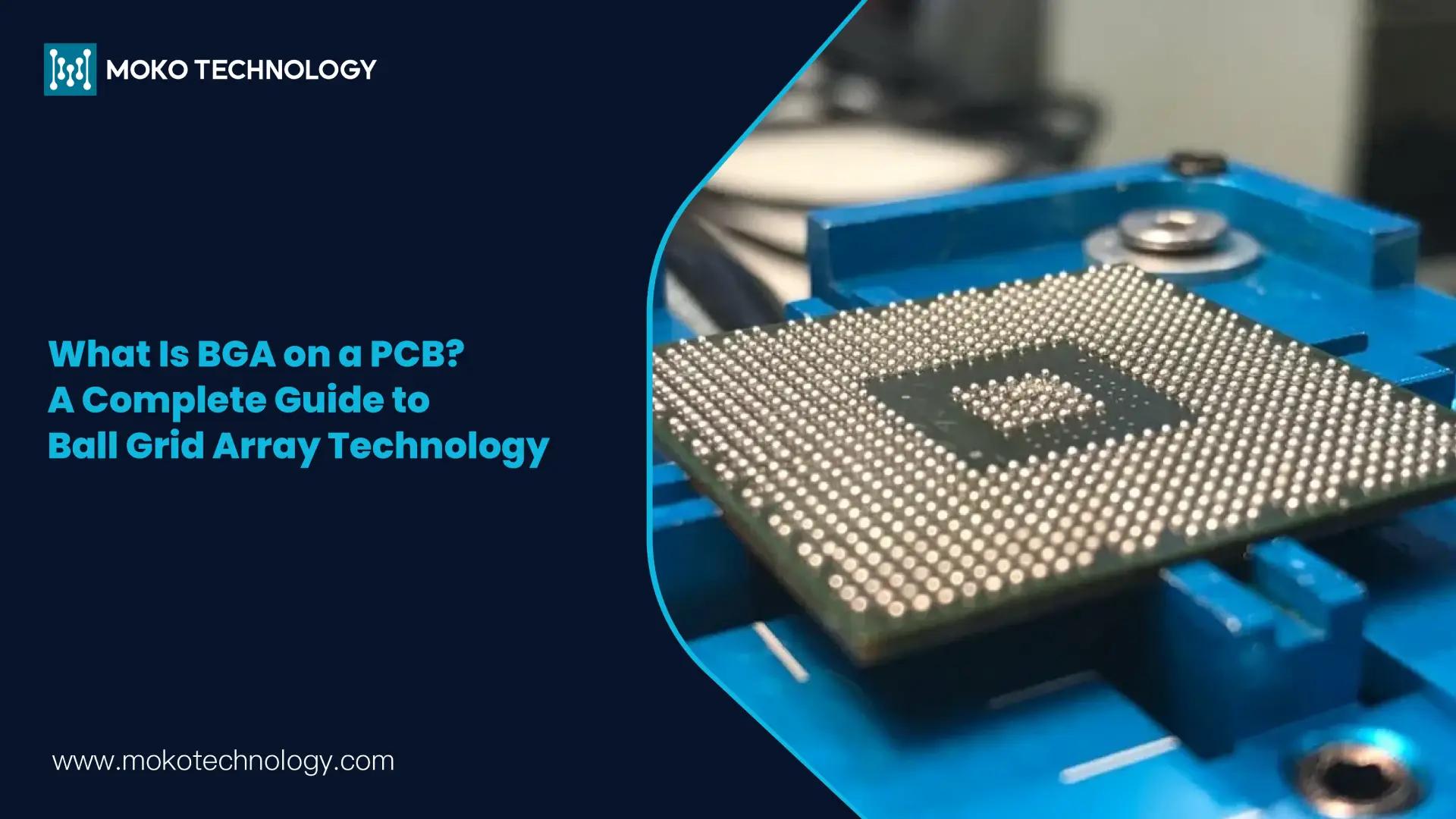
A Ball Grid Array is actually a type of surface mount packaging used in the manufacturing of integrated circuits. Unlike other packages which utilize leads extending from the periphery of the package, BGA uses a grid pattern of solder balls at the underside of the package. These solder balls used as the contact points between the chip and the printed circuit board.
6 Commonly Used BGA Package Types

In the market, there are various types of BGA packages used for different applications and requirements. Here, we will discuss six commonly used BGA package types:
PBGA(Plastic Ball Grid Array)
In PBGA, the substrate is BT resin/glass laminate, while the packaging material is plastic.The feature of this type of BGA package is that it does not require additional solder to connect the solder balls into the desired package. It is an affordable solution for a number of applications.
Ceramic BGA (CBGA)
CBGA is a kind of traditional ball grid array packaging type, which uses multilayer ceramic substrate as the base material. The metal lid is then soldered to the substrate using packaging solder to shield the chip, leads as well as the solder balls. The solder ball of it is mad from eutectic solder material, providing reliable connections between the substrate and the components.
Micro BGA (uBGA)
Micro BGA (µBGA) is an advanced Ball Grid Array packaging technology that takes up very little space. It offers much smaller chips; enhanced thermal management and increased density of data. As the name suggest, µBGA is primarily used in compact electronic devices and brings the much-needed enhanced performance in areas of size limitations.
Tape BGA (TBGA)
Tape Ball Grid Array (TBGA) is the kind of BGA packaging technique which uses the flexible tape instead of the rigid laminate. This can provide for light-weight and thin packaging with high density interconnects along with better thermal/ electrical characteristics.
Flip Chip Ball Grid Array (FC-BGA)
In FC-BGA, the integrated circuit is flipped so that it can be soldered onto the circuit board. This type of BGA package offers improved thermal and electrical performance as its solder balls connect to the PCB pads directly.
Package on Package (PoP)
In this kind of BGA package, many integrated circuits are stacked together. Each IC has its own ball grid array to enable components integration in a vertical way. It is widely used for applications that space is limited such as mobile devices.
| Type | Material | Solder Type | Key Features | Common Applications |
| PBGA | plastic | Leaded or lead-free | No additional solder needed for ball-to-package | Consumer electronics, low to mid-range applications |
| CBGA | ceramic | Eutectic | Long-standing type, protective lid | High-reliability applications, aerospace, military |
| uBGA | plastic | Not specified | Smaller size, better heat dissipation | High-frequency operations, compact electronic devices |
| TBGA | plastic | Not specified | Thinner, lighter, high-density interconnections | Portable electronics, smartphones, tablets |
| FC-BGA | Various | Direct to PCB | Enhanced thermal and electrical performance | High-performance processors, GPUs, network processors |
| PoP | Various | Multiple BGAs | Vertical integration, space-saving | Mobile devices, where space is premium, memory+processor stacks |
Advantages and Disadvantages of BGA Technology
Advantages
- Higher Density: Compared with traditional packages, BGAs allows more components be connected even in a small space, which is crucial for modern electronic devices.
- Improved Thermal Performance: The solder balls are arranged in a particular pattern, making them uniformly share heat, thus reducing the risk of overheating in some areas
- Reduced Inductance: In BGA, the shorter connect paths can minimize inductance, so as to enhance the signal integrity, which is particularly helpful at high frequencies.
- Better Reliability: When comparing with the leaded package, BGA provides greater reliability as there are fewer mechanical stresses it should bear during the thermal cycling process.
Disadvantages
- Inspection Challenges: It’s more difficult to inspect the quality of BGA’s solder joints as they are located at the underside of the package. Some soldering issues are hard to check only by naked eyes. We have to use specialized techniques like X-ray inspection.
- Repair Complexity: One of the downsides of BGA technique is the repair complexity. It is a time-consuming and costly process that requires professional tools such as BGA rework station.
- Highly Cautious Assembly: During the BGA soldering process, operators must be very careful to mount the components correctly, any mistake can affect the performance and even lead to poor connection.
How to Solder Ball Grid Array to Circuit Boards?

To ensure high reliability and minimize defect rates, it’s critical to strictly control the BGA soldering process. Here is a clear, key workflow and important technical considerations for BGA assembly.
Pre-Soldering Preparation
In this step, it’s important to be concerned with moisture control, especially for Plastic Ball Grid Array (PBGA), which is sensitive to humidity. If moisture is trapped inside, the rapid heating during reflow can cause the “popcorn effect,” damaging the chip or causing solder splashes.
When moisture-sensitive PBGAs are unsealed for more than 8 hours, they must be baked. The baking conditions are 120°C ± 5°C for 24 hours or 80°C ± 5°C for 48 hours.
Solder Paste Printing
The solder paste printing process significantly affects the soldering quality of Ball Grid Array. According to extensive statistical data, among the various BGA soldering processes, solder paste printing accounts for 64% of soldering defects. Components account for 6%, while component placement and reflow soldering each contribute 15%.
With excessive solder paste, solder bridging will occur. Conversely, if the solder paste is insufficient, defects such as cold joints may result.
BGA Pick and Place
Precise alignment is vital as BGA joints cannot be visually inspected after placement. Commonly, modern pick-and-place machines use vision systems to align the center of the solder balls with the center of the PCB pads. Once placed, the BGA should not be moved or adjusted manually, as this frequently causes bridging or insufficient solder.
Reflow Soldering
When the BGAs are completely placed on the board, then the PCB will be sent to the reflow oven. Under controlled heating, the solder paste melts, cools, and creates metallurgical bonding. The reflow profile must be strictly controlled to avoid issues such as voids, insufficient wetting, or excessive thermal stress on components.
Post-Soldering Inspection
Since Ball Grid Array joints are hidden under the package, traditional visual inspection is not enough. X-ray inspection, visual inspection, electrical testing, or other destructive methods are usually needed to check solder joint integrity. We will talk about this in the section that follows.
Top 8 BGA Defects You Should Know
The following are the common soldering defects encountered during the Ball Grid Array assembly process:
Cold Solder Joints: They typically appear dull and rough, with an uneven surface. And unmelted solder particles can be observed under a microscope.
Solder Bridging: Two or more neighboring solder balls are electrically connected unintentionally.
Insufficient wetting: The solder paste fails to properly wet the pad and form an alloy bond. Consequently, the BGA solder balls do not establish a proper electrical connection with the pads.
Missing Solder Balls: After reflow, one or more solder balls may be completely absent, leading to open connections.
Microcracks: It may happen at the solder joint interface or between the BGA chip and the solder ball.
Misalignment: The solder balls are not properly aligned with the PCB pads, causing positional offset. This can degrade the mechanical integrity of the solder joints.
Voiding: Bubbles trapped within the solder balls can cause the formation of internal voids.
Head-in-Pillow (HiP) Defects: The solder balls and solder paste have not fully or only partially fused, resulting in pillow-shaped solder joints. This defect is difficult to inspect, and the solder joints are prone to fracturing during subsequent use.
Ball Grid Array Inspection Techniques
Typically, Ball Grid Arrays possess hundreds of solder balls, and their solder joints may simultaneously exhibit multiple types of soldering defects. Below, we will introduce 5 testing techniques, which are generally divided into Non-Destructive Testing and Destructive Testing.
Non-Destructive Testing
Visual Inspection
Typically, it’s the first step, using the naked eye, magnifying glasses, or microscopes to inspect the outermost row of BGA solder joints. However, visual inspection is a labor-intensive task and cannot provide precise quantitative assessments. As a result, this method is generally unsuitable for high-quality and highly reliable products and large-scale inspection scenarios.
X-Ray Inspection
The “gold standard” for non-destructive Ball Grid Array (BGA) inspection is X-ray inspection. This method uses density differences to visualize the internal structure of the solder balls.
2D X-ray inspection should employ a 5-point inspection method, focusing on the four sides and the central five points of the device. At the same time, perform a rapid inspection of other areas. First, inspect the overall view of the BGA device, checking for defects like missing balls, misaligned balls, or solder bridging. Then, perform localized inspection, checking for solder Ball voiding or other solder ball anomalies.
Inspectors use 2D X-ray results (such as solder joint size, shape, and grayscale values) to determine whether 3D tomography is required. The judgment criteria are as follows: the BGA solder joints are normal in shape (circular) and exhibit no anomalies in terms of size or grayscale. Although 3D tomography can provide additional information about solder joints, the process can be expensive.
Electrical Testing
In electrical testing, we need to use specialized equipment such as a multimeter and flying probe tester to ascertain parameters, including resistance and continuity within BGA components. It discovers problems in connection performance and checks if solder joints are operating correctly.
Destructive Testing
Dye and Pry Test
This is a cost-effective destructive method that provides comprehensive information regarding the solder joint interface. A high-penetration dye is applied to the BGA. Then, the solder joint is pulled apart to observe the extent and distribution of internal cracking. Any area stained with dye indicates a pre-existing crack or separation.
Metallographic Cross-Section Analysis
This is the most precise method that can definitively confirm most defects. Information obtained through cross-sections can indicate whether defects are process-related or material-related. And then it helps determine at which step the correction needs to be addressed. However, metallographic testing also has certain limitations. The testing process is labor-intensive and requires relatively expensive equipment.
BGA Capabilities at TestPcbas
TestPcbas is proud of our sophisticated BGA assembly and inspection techniques. We use advanced facilities and modern technology, which enable us to guarantees both precision and quality at every assembly phase, enabling us to handle almost all BGA packages. Our collection of BGA services includes custom BGA assembly, highly advanced inspection techniques, engineering support, and rapid prototyping. If you require one-stop BGA PCB assembly services, do not hesitate to reach out to us.
BGA Package FAQs
- What are the key differences between BGA and LGA packages?
They differ in various aspects, including connection methods, pin density, thermal performance, etc.
BGA characteristics:
Uses solder balls to directly connect to the PCB
Supports high pin density
Inspection and rework are relatively difficult
Good heat dissipation through the PCB
LGA characteristics:
Uses flat pads to contact or socket
Enables easier replacement and upgradability
Simplifies inspection and rework
Good mechanical reliability, especially with the socket design
- Which IC package type—BGA, QFP, or QFN—poses the greatest challenges for PCB layout, and why?
BGA is more challenging, followed by QFN and QFP. Ball Grid Array (BGA) package poses the greatest challenges for significant design and production hurdles. Then comes QFN, which has a smaller size compared with QFP. This means it is more difficult to route.
- What is reballing in BGA assembly?
It means removing old, damaged, or defective solder balls from a BGA and replacing them with new ones. This process typically requires specialized equipment and materials, including stencils, solder balls, and a reflow oven or hot air gun.
- What are dog-bone fan-out and via-in-pad techniques in BGA PCB layout?
The dog-bone fan-out technique is a common and cost-effective option. A routing method where a short trace extends from a BGA pad to a nearby via (forming a “dog-bone” shape). Via-in-pad is an advanced technique, placing via directly on the BGA solder pad.


 Arabic
 Dutch
Dutch English
 French
 German
 Italian
 Japanese
 Korean
 Portuguese
 Russian
 Spanish